Semiconductor inspections
The SWIR band has been recognized as one of the best wavelength regions for semiconductor inspection. Whether it is for detecting cracks and defect on a wafer or solar cell panels, or for achieving a failure analysis of integrated circuits, InGaAs wavelength (900m- 1700nm) imaging device are suited for seeing through inside silicon.
Thermography.
Welding/additive manufacturing.
Lasers.
Microscopy.
Life science.
Microarray, genomics & biochip :
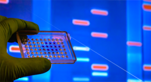
Biochip, genomics and microarray detection represent a mix of applications with varying needs of a scientific camera.
Some require long exposure, whereas others may prioritize high speed. Some may require high resolution and others might need low light imaging capabilities.